
Atomic Force Microscope
 It provides high resolution, three-dimensional imaging of the surface with the help of a needle tip sharpened down to atomic dimensions. Imaging is performed as a result of examining the interaction of the needle tip with the surface. Different needle tips are used for different purposes. Atomic force microscope can be used with three different techniques. These; The contact method in which the needle is applied by touching the surface, the non-contact method where the needle does not touch the surface, and the hitting method in which the needle is applied by striking the surface. In addition to visualizing the sample surfaces, phase, electrical conductivity and magnetic differences can also be detected.
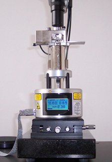
Instrument: Veeco MultiMode V
Specifications
| Model | Scanning Area | Vertical Analysis Area |
| AS-12 ("E") | 10µm x 10µm | 2,5µm |
| AS-130 ("J") | 125µm x 125µm | 5,0µm |
Sample Requirements
Specimens should be placed within a maximum diameter of 15 millimeters. The surface to be examined must be parallel to the mounting surface and smaller than 8 millimeters.The thickness of the sample must be equal in all directions and less than 1.5 mm.
Applications
Surface investigations of thin-film coatings.
Surface investigations of organic and inorganic materials.
Surface examinations can be made on the subjects of surface smoothness, phase differences, electrical conductivity differences and magnetic field direction differences.
It provides high resolution, three-dimensional imaging of the surface with the help of a needle tip sharpened down to atomic dimensions. Imaging is performed as a result of examining the interaction of the needle tip with the surface. Different needle tips are used for different purposes. Atomic force microscope can be used with three different techniques. These; The contact method in which the needle is applied by touching the surface, the non-contact method where the needle does not touch the surface, and the hitting method in which the needle is applied by striking the surface. In addition to visualizing the sample surfaces, phase, electrical conductivity and magnetic differences can also be detected.
Instrument: Veeco MultiMode V
Specifications
| Model | Scanning Area | Vertical Analysis Area |
| AS-12 ("E") | 10µm x 10µm | 2,5µm |
| AS-130 ("J") | 125µm x 125µm | 5,0µm |
Sample Requirements
Specimens should be placed within a maximum diameter of 15 millimeters. The surface to be examined must be parallel to the mounting surface and smaller than 8 millimeters.The thickness of the sample must be equal in all directions and less than 1.5 mm.
Applications
Surface investigations of thin-film coatings.
Surface investigations of organic and inorganic materials.
Surface examinations can be made on the subjects of surface smoothness, phase differences, electrical conductivity differences and magnetic field direction differences.